As a result, the electromagnetic emission of modern IC sand their electromagnetic susceptibility have become a major issue in the design of electronics-based systems. In this context, engineers are increasingly required to ensure that their developed products function satisfactorily in their electromagnetic environment, i.e. that they are not functionally affected by electromagnetic interferences, but also that they do not negatively influence other devices through their electromagnetic emission.
But before we get into that, we should think about why electromagnetic compatibility of electronic devices and systems concerns us all and why this topic should be important for everyone. If the video that we are watching on our tablet gets stuck due to an electrostatic discharge that occurs as our fingers approach the tablet, it is annoying in most cases, but usually not life-threatening.
However, the situation might be different when electromagnetic interference occurs during the operation of avionics, automotive or industrial applications. Here, interference can very often have life-threatening consequences.
An example from the automotive sector should illustrate this. Airbag systems are designed to protect passengers in the event of an accident. The heart of the airbag system is the so-called airbag control unit, which usually consists of an “application-specific integrated circuit” or ASIC that monitors the signals of the crash sensors in the vehicle to determine whether the airbags need to be triggered or not. The prerequisite, however, is that the ASIC is not functionally influenced by electromagnetic interferences. Ensuring the EMCand at the same time the functional safety of modern airbag systems under all circumstances is difficult in many cases, as different types of interference can occur and a complete test of the ACU at all levels, i.e. from AISC, the control module to the finished vehicle, is usually very extensive.
Automakers and airbag suppliers have known about such kinds of interferences and the consequent malfunctioning units that caused airbags in certain vehicles to fail to deploy and have left passengers without expected protection during a crash for many years. But measures are usually not taken until years later, when the first fatalities associated with the failure of electronic systems have occurred.
The most widespread EMI problem in the media started in 2016 when many automakers began recalling millions of cars for airbag malfunctions [1]. The National Highway Traffic Safety Administration announced at the time that this airbag problem involved six different car companies and affected an estimated 12.3 million vehicles. But this was by no means the largest airbag recall operation in recent years [2].
The demand for robust electronic systems capable of operating satisfactorily in their electromagnetic environment is increasing, and for safe operation it is very important that all designed functions work properly and sensed signals are reliable and accurate. Many EMC problems of electronic systems can be attributed to interference issues caused by the low immunity of the ICs that are used. Therefore it is important to solve EMC problems directly at their source.
Ensuring EMC
Well, one of the approaches is that great attention must be paid to EMC behavior during the design of the particular IC. Especially with the increasing density of components in modern ICs, their emission and immunity performance has become a design factor to be considered.
Direct Power Injection
CMOS operational amplifiers that are built into automotive systems such as smart power switches are very often used as sensor interfaces as part of their implemented electronic sensor systems. Often their power supply and inputs are directly connected to the wiring harness and are therefore particularly susceptible to any kind of interference received by the cables that can act as receiving antennas. As a consequence operational amplifiers can be heavily disturbed and must therefore withstand a high level of electromagnetic interference [3].
Figure 1 shows a block diagram of the EMC test bench that can be used to characterize the susceptibility of operational amplifiers in the EMC lab of the Institute of Electronics. The interference signal is fed into one of the inputs of the operational amplifier at wafer level by means of special feed heads (GSG probe) via a radio-frequency generator. The bias T is used to decouple the DC path (VIN_nom) from the AC path (Vemi(t)), while the 20dB attenuator counteracts the reflections that occur along the injection path due to impedance mismatch. The ammeter monitors the bias current (Ibias) used to bias the amplifier. The robustness of the operational amplifier is monitored by a multimeter which measures and averages the output voltage VOUT that should not change due to EMI. During characterization, the forward power of the interference signal is gradually increased at the start frequency (e.g. 1MHz) until the monitored output voltage exceeds a predefined limit. Then the frequency of the interference signal is increased by one step and the procedure is started again. This is done until the stop frequency is reached (e.g. 1GHz). The resulting diagram is called DPI-characteristic of the operational amplifiers input over the frequency range of interest. If this characteristic is above a given limit, the operational amplifier is classified as robust; otherwise the designer is given some hints as to the frequency range in which the circuit needs to be improved.
Surface scan
Many different techniques are currently available to characterize the electromagnetic emission of ICs. With the so-called surface scan method that is described in the international standard IEC 61967-3, IC designers have a very useful characterization method at their disposal in order to find the sources of the electromagnetic emission directly on the surface of their ICs [4], [5]. This method is based on the measurement of electric and magnetic near-fields at the surface of IC packages or microchips. During measurement the device under test is powered up and fully operational while the generated near-field emission spectrum is measured by automatically moving a near-field probe over the DUT. This technique enables the distribution to be visualized over a wide frequency range of near-fields emitting from the surface of the DUT.

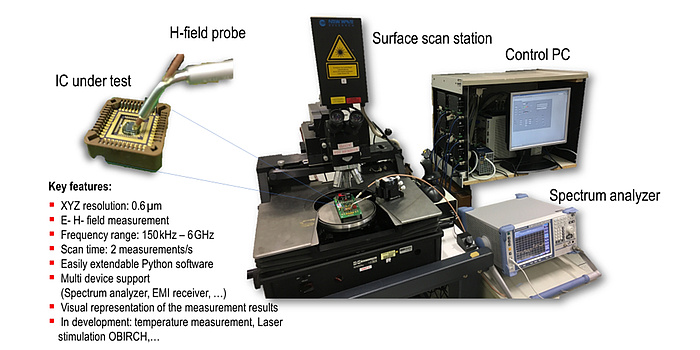
Figure 2: Surface scanning system at the Institute of Electronics.
Figure 2 shows the surface scan system of the Institute of Electronics which consists of a micromanipulation (wafer prober) that is equipped with stepper motors to control the movement of the DUT in relation to a specially designed magnetic near-filed probe that is connected via an amplifier to a spectrum analyzer.

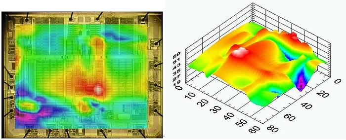
Figure 3: Surface scan of the magnetic near field of an IC (white/ red shows high, while blue/purple low magnetic fields).
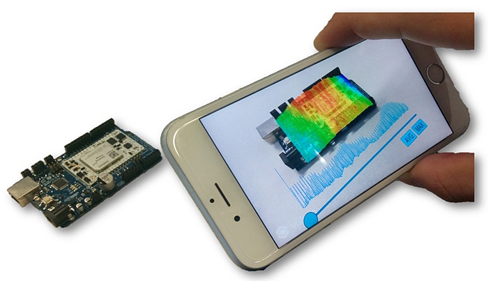
The magnetic near-fields at the surface of an IC under test are shown in Figure 3 in a color-coded representation that is superimposed on the photo of the microchip. This picture shows different areas with higher (white, red) and lower magnetic fields (blue, violet) and gives the IC designers a good overview of the locations of the emission sources and thereby helps to identify and analyze emission hotspots. In addition, an augmented reality app running on a smartphone or tablet can be used to superimpose the corresponding measurement results semi-transparently on a DUTand thus allows the observation of the field distributions from different directions. Figure 4 shows an example of such an augmented reality application.

Figure 4: Visualization of the near-fields by using an augmented reality app.
- Seeger Weiss LLP, “ZF-TRW Airbag Safety Investigation” https://www.consumersafetyguide. com/automotive/zf-trw-airbag-safety/
- Consumer Reports, “Takata Airbag Recall - Everything You Need to Know”, 2018, https:// www.consumerreports.org/cro/news/2016/05/everything-you-need-to-know-about-the-takata-air-bag-recall/index.htm
- Andrea Lavarda, “EMI susceptibility of offset compensated CMOS operational amplifiers,” PhD thesis, Graz University of Technologies, Graz, November 2018
- IEC TS 61967-3:2014, “Integrated circuits - Measurement of electromagnetic emissions - Part 3: Measurement of radiated emissions - Surface scan method,” TC 47/SC 47A, Ed. 2.0, International Electrotechnical Commission, 2014-08-25
- Bernd Deutschmann, Andreas Gleinser, Philipp Reitter, ”Electromagnetic Emission Scanning at the Surface of ICs,” Proc. of 15th EMV-Fachta-gung, OVE Schriftenreihe Nr. 87, 26 Apr 2017
![© Andrea Lavarda [3] An electronic circuit.](https://www.tugraz.at/fileadmin/_processed_/6/e/csm_icc1_by_Andrea_Lavarda_1d531abbff.jpg)
